WaferGrid Technologies Pte Ltd | Semiconductor Test & Measurement
Semiconductor Test and Measurement
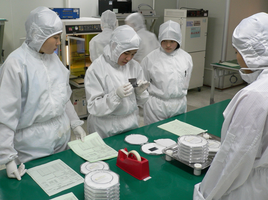
WaferGrid Technologies Pte Ltd combines contact hardware, automation software, cryogenic measurement capability, and applications engineering to improve test confidence at every stage of the IC lifecycle.
Custom MEMS and vertical probe-card architectures for fine-pitch, high-parallelism test.
Learn More
A complete application map from first silicon characterization to mature high-volume sort.
Learn More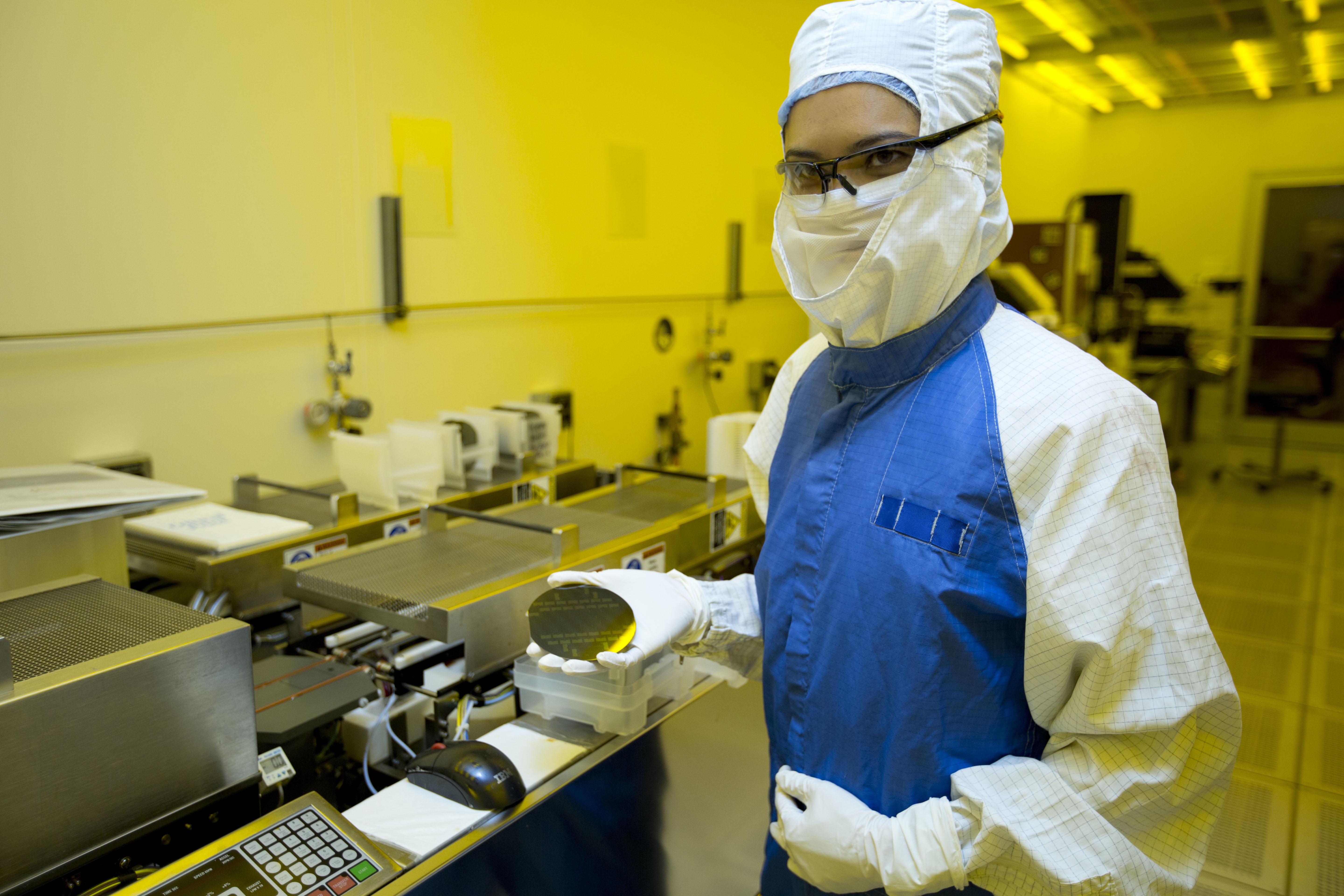
Regional sales, field service, applications engineering, logistics, and repair support.
Learn More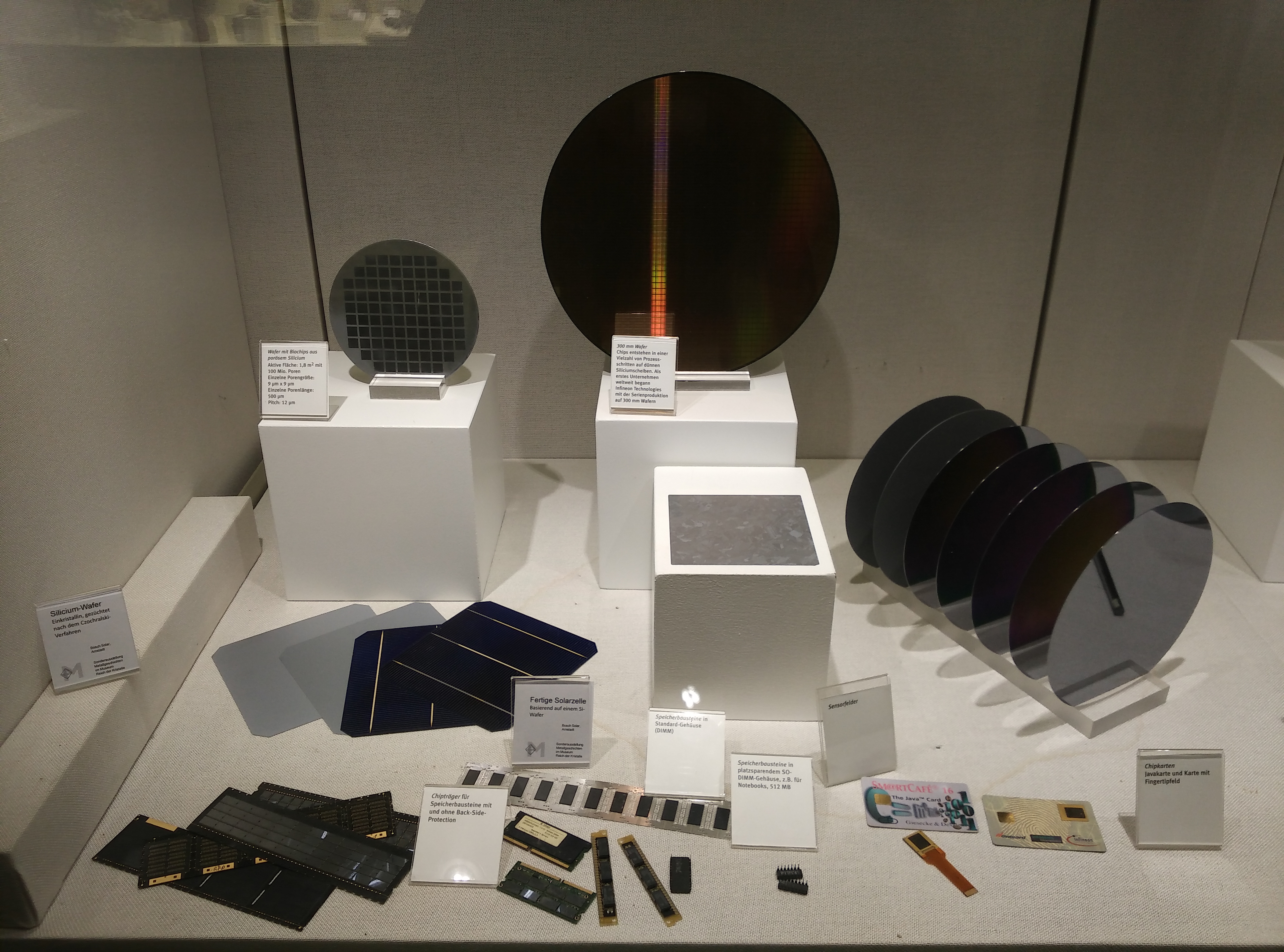
Meet the WaferGrid Technologies Pte Ltd team, our operating model, and our growing global footprint.
Learn MoreOur platform portfolio is designed around the practical work of semiconductor teams: characterize early devices, validate designs, qualify processes, and scale reliable production test.
Focused solutions for the technologies shaping the next generation of computing, connectivity, mobility, and secure systems.
Thermal-aware probing for high-current logic, chiplets, and advanced package bring-up.
Learn More
High-frequency measurement fixtures, calibration methods, and production-ready RF contact.
Learn More
Low-temperature probing workflows for superconducting, spin, and photonic quantum devices.
Learn More